Pinout
Overview
The moddoMOUSE Main Board exposes two expansion connectors on each side: one on the left edge and one on the right edge. Together they form the Front Board connector (J30 + J31) and the Back Board connector (J40 + J41). The diagram below shows all pins available on each connector, along with the onboard components visible from the top/dbottom of the board.
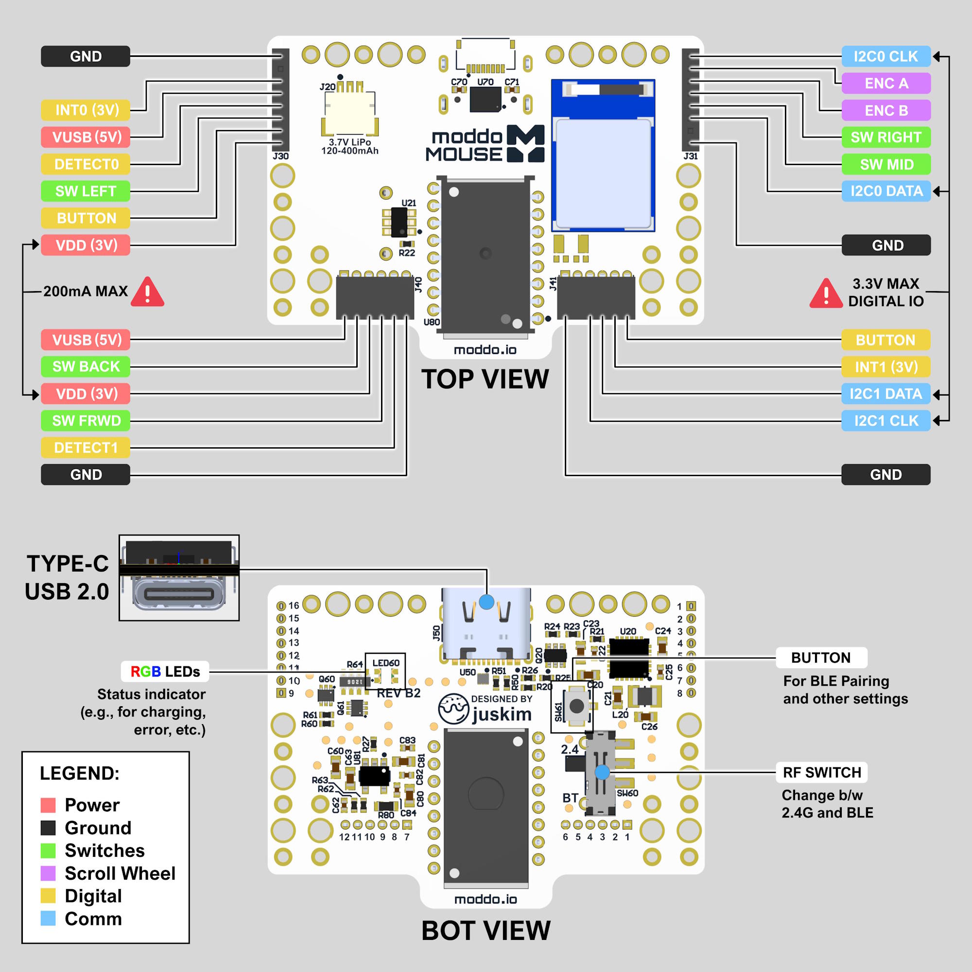
The pins are color-coded by type:
- 🔴 Power — Supply voltage pins (VDD, VUSB)
- ⚫ Ground — GND reference
- 🟢 Switches — Direct switch connections to the Main Board
- 🟣 Scroll Wheel — Encoder signals for vertical scroll wheel input
- 🟡 Digital — General purpose digital I/O (DETECT, BUTTON, INT)
- 🔵 Comm — Communication bus pins (I2C SDA/SCL)
⚠️ All digital and communication pins are 3.3V logic. Do not drive them above 3.3V or you risk damaging the Main Board. VDD is rated at 200mA max across both expansion connectors. Keep your expansion board's total current draw within this limit!
Front Board Connector (J30 / J31)
The Front Board connectors are located on the left (J30) and right (J31) edges of the Main Board. They expose the I2C0 bus, front-side switch signals, scroll wheel encoder, and power.
| Pin | Type | Description |
|---|---|---|
| VDD (3V) | Power | 3V power supply from the Main Board (200mA max shared) |
| VUSB (5V) | Power | 5V USB supply, only present when USB is connected |
| GND | Ground | Ground |
| I2C0 SDA | Comm | I2C0 data line (3.3V max) |
| I2C0 CLK | Comm | I2C0 clock line (3.3V max) |
| INT0 (3V) | Comm | Interrupt output from the Main Board (active high, 3.3V) |
| SW LEFT | Switch | Left mouse button switch |
| SW RIGHT | Switch | Right mouse button switch |
| SW MID | Switch | Middle mouse button switch |
| ENC A | Scroll Wheel | Scroll wheel encoder channel A |
| ENC B | Scroll Wheel | Scroll wheel encoder channel B |
| DETECT0 | Digital | Front Expansion board detect pin |
| BUTTON | Digital | Shared button input |
Back Board Connector (J40 / J41)
The Back Board connectors are located on the left (J40) and right (J41) edges of the Main Board. They expose the I2C1 bus, back-side switch signals, and power.
| Pin | Type | Description |
|---|---|---|
| VDD (3V) | Power | 3V power supply from the Main Board (200mA max shared) |
| VUSB (5V) | Power | 5V USB supply, only present when USB is connected |
| GND | Ground | Ground |
| I2C1 DATA | Comm | I2C1 data line (3.3V max) |
| I2C1 CLK | Comm | I2C1 clock line (3.3V max) |
| INT1 (3V) | Comm | Interrupt output from the Main Board (active high, 3.3V) |
| SW BACK | Switch | Backward mouse button switch |
| SW FRWD | Switch | Forward mouse button switch |
| DETECT1 | Digital | Back Expansion board detect pin |
| BUTTON | Digital | Shared button input |
Onboard Components (Bottom View)
The bottom of the Main Board exposes several onboard components relevant to end users and expansion board designers.
| Component | Description |
|---|---|
| USB-C (USB 2.0) | Used for wired HID mode and battery charging |
| RGB LEDs | Status indicator for charging state, errors, pairing mode, and other system events |
| BUTTON | Used for BLE pairing and other settings |
| RF SWITCH | Physical switch to toggle between 2.4GHz wireless and Bluetooth modes |